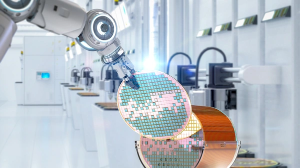
The Importance of Advanced Semiconductor Testing
The semiconductor industry is rapidly evolving, with increasing demand for advanced chips and complex semiconductor devices. Advanced semiconductor testing software is crucial for ensuring the reliability and performance of these devices, driven by market demand.
Contact us for a free quote in 12 hours and meet with one of our engineers.
Next-generation semiconductor testing software solutions are necessary to meet the challenges of testing advanced chips.
The importance of advanced semiconductor testing cannot be overstated, as it directly impacts the quality and reliability of semiconductor devices.
Semiconductor Test Solutions Overview
- Semiconductor test solutions are designed to meet the specific needs of the semiconductor industry.
- These solutions provide a comprehensive approach to testing semiconductor devices, from wafer testing to final testing.
- Semiconductor test solutions include a broad range of test tools and technologies, such as automated test equipment (ATE) and artificial intelligence (AI).
- The goal of semiconductor test solutions is to ensure the quality and reliability of semiconductor devices.
Stages of Semiconductor Testing
Wafer Testing
Wafer testing is the first stage of semiconductor testing, where the semiconductor wafer is tested for defects and failures. Wafer testing is critical for identifying defects early in the manufacturing process, reducing waste and improving yield.
Advanced wafer testing solutions use AI and machine learning to improve test efficiency and accuracy, supported by well-designed test programs. Wafer testing is a crucial step in ensuring the quality and reliability of semiconductor devices.
Package Testing
Package testing is the second stage of semiconductor testing, where the packaged semiconductor device is tested for electrical, mechanical, and thermal performance.
Package testing is designed to ensure that the packaged device meets the required specifications and performance criteria.

Final Testing
Final testing is the third and final stage of semiconductor testing, where the packaged semiconductor device is tested in a system similar to the one it will be used in.
Final testing is designed to ensure that the device functions correctly in real-world applications. Advanced final testing solutions use AI and machine learning to improve test efficiency and accuracy, significantly reducing test time.
Applications of Semiconductor Testing
Semiconductor testing is used in a wide range of applications, including consumer electronics, automotive, and industrial. The increasing demand for advanced chips and complex semiconductor devices, including mixed signal systems, has driven the need for more sophisticated semiconductor testing solutions. Semiconductor testing is critical for ensuring the reliability and performance of semiconductor devices in various operating conditions.
The applications of semiconductor testing continue to expand as the semiconductor industry evolves.
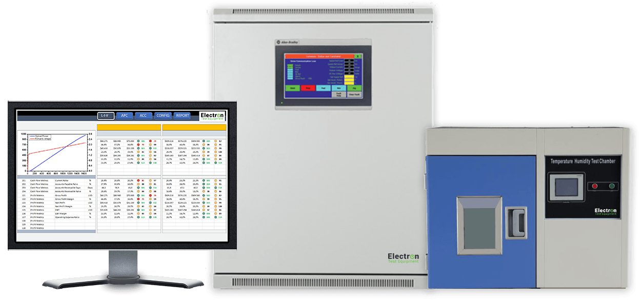
Measurement Solutions for Semiconductor Devices
Measurement solutions for semiconductor devices are designed to provide accurate and reliable measurements of device performance. The increasing demand for advanced chips and complex semiconductor devices has driven the need for more sophisticated measurement solutions.
Technologies for Semiconductor Testing
Artificial Intelligence in Semiconductor Testing
- Artificial intelligence (AI) is being increasingly used in semiconductor testing to improve test efficiency and accuracy.
- AI-powered test solutions can analyze large amounts of data and identify patterns and trends that may not be apparent to human testers.
- AI is critical for ensuring the quality and reliability of semiconductor devices in the age of big data.
- The use of AI in semiconductor testing is expected to continue to grow in the coming years.
Next-Generation Display Testing
- Next-generation display testing is critical for ensuring the quality and reliability of display devices.
- Advanced display testing solutions use high-speed test tools and AI to improve test efficiency and accuracy.
- The increasing demand for high-resolution displays has driven the need for more sophisticated display testing solutions.
- Next-generation display testing is critical for ensuring the quality and reliability of display devices.
Emerging Trends in Semiconductor Testing
The semiconductor industry is in a constant state of flux, and testing methodologies are evolving to keep pace. One of the most significant emerging trends is the increasing use of artificial intelligence (AI) and machine learning (ML) to enhance test efficiency and accuracy. These technologies can analyze vast amounts of data, identify patterns, and predict potential failures, making the testing process more robust and reliable.
Another notable trend is the growing demand for testing wide bandgap semiconductors, such as silicon carbide (SiC) and gallium nitride (GaN). These materials offer superior performance in high-power and high-frequency applications but require specialized test solutions due to their unique properties. As the market for these advanced materials expands, so does the need for tailored testing methodologies.
Additionally, the increasing complexity of semiconductor devices is driving the development of more advanced test tools and techniques. Innovations like 3D stacked die testing and wafer-level testing are becoming more prevalent, allowing for more comprehensive and accurate assessments of device performance. These advancements are crucial for meeting the stringent quality and reliability standards of modern semiconductor devices.
Challenges in Semiconductor Testing
Semiconductor testing is a multifaceted and challenging process, with several hurdles that must be overcome to ensure the quality and reliability of semiconductor devices. One of the primary challenges is the escalating complexity of these devices. As semiconductor technology advances, the intricacy of the circuits and components increases, necessitating more sophisticated test tools and techniques.
Wafer-level testing presents another significant challenge. This early stage of testing requires specialized equipment and methodologies to identify defects and failures before the devices are packaged. Ensuring accuracy at this stage is critical for reducing waste and improving overall yield.

The growing demand for wide bandgap semiconductors, such as SiC and GaN, adds another layer of complexity. These materials require unique testing solutions due to their distinct electrical properties and operating conditions. Developing and implementing these specialized test solutions is essential for ensuring the performance and reliability of these advanced devices.
Furthermore, the integration of AI and ML into semiconductor testing introduces its own set of challenges. These technologies require specialized expertise and equipment to be effectively utilized. Ensuring that testing personnel are adequately trained and that the necessary infrastructure is in place is crucial for leveraging the full potential of AI and ML in semiconductor testing.
Environmental Impact of Semiconductor Testing
The semiconductor industry, while driving technological innovation, also has a significant environmental footprint. The production and disposal of semiconductor devices consume substantial amounts of energy and resources, and the testing process itself generates waste and emissions. Addressing these environmental impacts is becoming increasingly important as the industry grows.
To mitigate this impact, the semiconductor industry is adopting more sustainable practices. Efforts to reduce energy consumption during testing, use environmentally friendly materials, and minimize waste are gaining traction. For instance, optimizing test processes through AI and ML can significantly reduce the need for physical prototypes, thereby cutting down on material waste and emissions.
Moreover, the development of more efficient test solutions plays a crucial role in reducing the environmental impact of semiconductor testing. By improving test efficiency and accuracy of Photodiode Reliability & Accelerated Life Testing, these solutions can help lower the overall energy consumption. As the industry continues to innovate, the focus on sustainability will be essential for balancing technological advancement with environmental responsibility.
Yield Enhancement and Quality Improvement
- Yield enhancement and quality improvement are critical for ensuring the quality and reliability of semiconductor devices.
- Advanced semiconductor testing solutions can help improve yield and quality by identifying defects and failures early in the manufacturing process.
- The use of AI and machine learning in semiconductor testing can help improve test efficiency and accuracy, leading to improved yield and quality.
- Yield enhancement and quality improvement are critical for ensuring the quality and reliability of semiconductor devices.
Industry Insights and Resources
- The semiconductor industry is rapidly evolving, with increasing demand for advanced chips and complex semiconductor devices.
- Industry insights and resources are critical for staying up-to-date with the latest trends and technologies in semiconductor testing.
- The use of AI and machine learning in semiconductor testing is expected to continue to grow in the coming years.
- Industry insights and resources are critical for ensuring the quality and reliability of semiconductor devices.